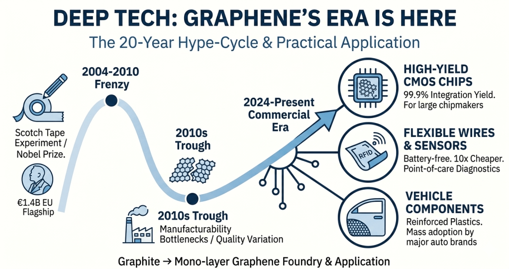
The 20-year hype-cycle of a miracle material
Twenty years ago I read a piece in Science magazine about a single-atom-thick material that was stronger than steel, could conduct electricity, flex like a film, and sense almost anything.
Graphene. It read like science fiction.
Last week, I was coaching two graphene companies on their pitch to three semiconductor powerhouses at the Hello Tomorrow Summit Deep Tech Days.
The science fiction is now a pitch deck, backed by practical applications for this miracle material.
The Hype-Cycle
For anyone familiar with the Gartner hype cycle (Innovation, peak of inflated expectations, trough of disillusionment, slope of enlightenment, plateau of productivity) – graphene is a textbook case. It climbed fast and fell hard.
Here is what that 20-year deep-tech hype-cycle looks like:
Innovation – Andre Geim and Konstantin Novoselov discovered graphene on a Friday night in Manchester in 2004, using a block of graphite and ordinary Scotch tape. They were awarded the Nobel Prize six years later.
Frenzy – Within months of the prize, the European Union had committed €1.4 billion to a Graphene Flagship program. Billions more followed globally.
Fall – Then came the trough. Geim says of that period: “Expectations were very, very high. The companies I was involved in were mostly based on hype.”
The problem was not the properties. The problem was manufacturability. Chemical vapor deposition — the process developed in 2009 to grow graphene — produced a jigsaw of graphene crystals, and the seams between them dramatically affect performance. Getting the graphene off the copper foil it grows on and onto a device without tearing, wrinkling, or contaminating it turned out to be enormously difficult. Quality varied wildly between batches, between suppliers, between labs. And integration with semiconductor “clean room” manufacturing was challenging.
The Commercial Era
Finally, practical applications and initial commercialization is starting to happen. Ford has put graphene-reinforced components into over 5 million vehicles. Huawei uses graphene oxide as a heat spreader in millions of smartphones. INBRAIN Neuroelectronics is in clinical trials with graphene-based brain implants. Black Semiconductor raised €250M+ for graphene optical chips.
Natasha Conway of Paragraf said it better than I can: “It’s gone up the hill, down into the big valley – and now it’s coming out as people see that it really does have value.”
That sentence is the starting gun for the commercial era. IDTechEx estimates the graphene materials market at roughly $150 million per year today, rising to $1.6 billion by 2034. But critically, monolayer graphene – the real thing, not the various graphene-adjacent materials that have populated the market – is poised to grow its share of that figure as the transfer and integration problems that blocked it for a decade are finally being solved.
Real-World Application
The two companies I coached for Hello Tomorrow are proof-points that we are just entering the practical commercialization window.
→ Grapheal (Grenoble, CNRS spin-out) – flexible graphene sensors on polymer film. Battery-free. NFC-powered. Smartphone-readable. 10x cheaper than silicon. Wound monitoring patches, point-of-care diagnostics, industrial gas sensing. 22 patents. France 2030 laureate.
My coaching to Grapheal going into meetings with potential corporate partners – lead with the outcome. Battery-free. Wireless. AI-ready sensing at one-tenth the cost of silicon. Sensing AI-ready edge data is a product fit hiding in plain sight.
→ Graphenea (San Sebastián) – the world’s only dedicated graphene foundry. 99.9% device yield in CMOS-integrated graphene arrays. That yield number is key. CMOS is short for Complementary Metal-Oxide-Semiconductor, the dominant and highly efficient fabrication process used to create modern integrated circuits. Integration yield is the gating question for every chipmaker evaluating whether to adopt a new material. As their CSO Amaia Zurutuza told Science magazine: “Transfer is not the main bottleneck anymore.”
My coaching: the 99.9% yield CMOS integration data is the entire opening. Then propose a joint development agreement. Biosensing is the near-term entry point; Physical AI sensing is the longer-term play.
Two graphene companies in the same Hello Tomorrow cohort is not coincidence. The EIC Accelerator has €634 million allocated for 2026 for exactly this class of company: hardware-rooted, patent-protected, commercially ready.
The Twenty-Year Bet
In investor terms, graphene was a twenty-year research project paid for by governments, universities, and patient capital. The Graphene Flagship spent €1.4 billion. The UK spent £61 million on the NGI. Hundreds of companies burned through VC dollars on applications that were three or four technology generations too early.
That spending was not wasted. The founders I coached are the beneficiaries of a twenty-year R&D subsidy. The learning curve has been climbed. The transfer problem is no longer the main bottleneck.
This is where venture returns can be made.
The material that felt like science fiction is now a pitch deck for some of the world’s largest chipmakers. A Scotch tape experiment, run on a Friday night in 2004, is their origin story.
The twenty-year arc of deep tech, up close, looks like this.
P.S. After my coaching calls last week, I searched for the original article I read 20 years ago and instead found this excellent piece on graphene’s history by Mark Peplow at Science.org. His article is a primary source for these musings and well worth a read.
#DeepTech #GrapheneSensors #EICAccelerator #StartupEurope #VentureCapital #SemiconductorInnovation #EdgeAI #HelloTomorrow #Graphenea #Grapheal

